| CPC H01L 24/45 (2013.01) [H01L 24/03 (2013.01); H01L 24/05 (2013.01); H01L 24/08 (2013.01); H01L 24/80 (2013.01); H01L 25/0657 (2013.01); H01L 25/18 (2013.01); H01L 25/50 (2013.01); H01L 2224/03614 (2013.01); H01L 2224/04042 (2013.01); H01L 2224/05017 (2013.01); H01L 2224/08145 (2013.01); H01L 2224/4502 (2013.01); H01L 2224/45124 (2013.01); H01L 2224/45147 (2013.01); H01L 2224/80895 (2013.01); H01L 2224/80896 (2013.01); H01L 2924/1431 (2013.01); H01L 2924/1444 (2013.01); H01L 2924/14511 (2013.01)] | 26 Claims |
|
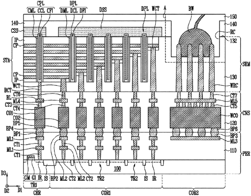
1. A semiconductor device comprising:
a first insulating layer;
wire contacts spaced apart from each other by the first insulating layer; and
a bonding wire connected to the wire contacts,
wherein each of the wire contacts includes a base part in the first insulating layer and a protrusion part protruding from inside to outside the first insulating layer, and
wherein the protrusion parts of the wire contacts are in direct contact with the bonding wire.
|