| CPC H01L 24/14 (2013.01) [H01L 23/528 (2013.01); H01L 23/53214 (2013.01); H01L 23/53228 (2013.01); H01L 23/562 (2013.01)] | 19 Claims |
|
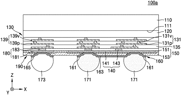
1. A semiconductor chip comprising:
a semiconductor substrate;
a back end of line (BEOL) structure on a first surface of the semiconductor substrate, the BEOL structure including a conductive connection structure and an interlayer insulating layer covering the conductive connection structure;
a conductive reinforcing layer on the BEOL structure,
the conductive reinforcing layer being electrically connected to the conductive connection structure and having a plate shape extending parallel to the first surface of the semiconductor substrate;
a cover insulating layer covering the conductive reinforcing layer;
an under bump metal (UBM) layer including a plurality of pad connection portions connected to the conductive reinforcing layer through openings in the cover insulating layer; and
a plurality of first connection bumps on the plurality of pad connection portions of the UBM layer, the plurality of first connection bumps being spaced apart from each other,
the plurality of first connection bumps being electrically connected to one another through the conductive reinforcing layer such that the plurality of first connection bumps are electrically connected to the conductive connection structure of the BEOL structure through the conductive reinforcing layer, and overlapping the conductive reinforcing layer in a direction perpendicular to the first surface of the semiconductor substrate,
wherein a material of the conductive reinforcing layer is different than a material of the UBM layer and a material of the conductive connection structure of the BEOL structure.
|