| CPC H01L 24/02 (2013.01) [H01L 24/05 (2013.01); H01L 24/13 (2013.01); H01L 24/14 (2013.01); H01L 24/73 (2013.01); H01L 24/92 (2013.01); H01L 2224/02311 (2013.01); H01L 2224/02371 (2013.01); H01L 2224/0401 (2013.01); H01L 2224/05024 (2013.01); H01L 2224/05124 (2013.01); H01L 2224/05147 (2013.01); H01L 2224/05155 (2013.01); H01L 2224/05166 (2013.01); H01L 2224/05171 (2013.01); H01L 2224/13026 (2013.01); H01L 2224/14183 (2013.01); H01L 2224/73253 (2013.01); H01L 2224/92225 (2013.01)] | 20 Claims |
|
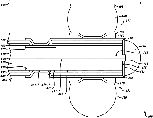
1. A device, comprising:
a semiconductor die including a first surface, a second surface opposite to the first surface, a first sidewall surface transverse to the first and second surfaces;
a contact pad exposed from the first surface;
a first dielectric layer on the contact pad and extending from the contact pad to the first sidewall surface, the first dielectric layer including a second sidewall surface coplanar with the first sidewall surface;
a second dielectric layer on the contact pad and extending from the contact pad to the first and second sidewall surfaces, the second dielectric layer having a third sidewall surface coplanar with the first and second sidewall surfaces, the second dielectric layer having a surface facing away from the semiconductor die;
a mold protection layer on and covering the first, second, and third sidewall surfaces, the mold protection layer having an end surface facing away from the semiconductor die and a fourth sidewall surface transverse to the end surface of the mold protection layer;
a redistribution layer on the contact pad and extending from the contact pad to the mold protection layer, the redistribution layer covering the surface of the dielectric layer, the end surface of the mold protection layer, and the sidewall surface of the mold protection layer; and
a third dielectric layer on the redistribution layer and on the second dielectric layer, the third dielectric layer overlaps the contact pad and the first dielectric layer.
|