| CPC H01L 23/66 (2013.01) [H01L 21/4853 (2013.01); H01L 21/4857 (2013.01); H01L 21/561 (2013.01); H01L 21/565 (2013.01); H01L 21/568 (2013.01); H01L 21/6835 (2013.01); H01L 21/6836 (2013.01); H01L 21/78 (2013.01); H01L 23/3114 (2013.01); H01L 23/3128 (2013.01); H01L 23/5383 (2013.01); H01L 23/5384 (2013.01); H01L 23/5386 (2013.01); H01L 23/5389 (2013.01); H01L 23/552 (2013.01); H01L 24/19 (2013.01); H01L 24/20 (2013.01); H01L 24/96 (2013.01); H01L 25/105 (2013.01); H01L 25/50 (2013.01); H01P 3/003 (2013.01); H01Q 1/2283 (2013.01); H01Q 1/38 (2013.01); H01Q 9/0457 (2013.01); H01L 21/486 (2013.01); H01L 2221/68331 (2013.01); H01L 2221/68359 (2013.01); H01L 2221/68372 (2013.01); H01L 2223/6616 (2013.01); H01L 2223/6627 (2013.01); H01L 2223/6677 (2013.01); H01L 2224/214 (2013.01); H01L 2224/95001 (2013.01); H01L 2224/97 (2013.01); H01L 2225/1035 (2013.01); H01L 2225/1058 (2013.01); H01L 2924/3025 (2013.01); H01Q 21/065 (2013.01)] | 20 Claims |
|
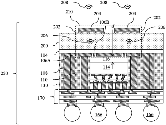
1. A method comprising:
forming a ground element and a feed line of an antenna over a first side of a first dielectric layer, the first dielectric layer being on a substrate;
placing a dielectric feature and a radio frequency chip over the ground element and the feed line, wherein a portion of the dielectric feature is interposed between the radio frequency chip and the ground element;
encapsulating the radio frequency chip and the dielectric feature in an encapsulant, wherein the encapsulant is external to the radio frequency chip;
detaching the substrate from the first dielectric layer;
forming a second dielectric layer on a second side of the first dielectric layer, the second side being opposite the first side; and
attaching a radiating element of the antenna to the second dielectric layer.
|