| CPC H01L 23/585 (2013.01) [H01L 23/492 (2013.01); H01L 23/564 (2013.01); H01L 24/05 (2013.01); H01L 24/32 (2013.01); H01L 24/48 (2013.01); H01L 24/73 (2013.01); H01L 29/0684 (2013.01); H01L 21/0217 (2013.01); H01L 21/0254 (2013.01); H01L 21/0272 (2013.01); H01L 21/0277 (2013.01); H01L 21/02211 (2013.01); H01L 21/02274 (2013.01); H01L 21/2654 (2013.01); H01L 21/31144 (2013.01); H01L 21/32139 (2013.01); H01L 24/03 (2013.01); H01L 29/2003 (2013.01); H01L 29/205 (2013.01); H01L 29/402 (2013.01); H01L 29/42316 (2013.01); H01L 29/452 (2013.01); H01L 29/475 (2013.01); H01L 29/66462 (2013.01); H01L 29/7786 (2013.01); H01L 2224/0345 (2013.01); H01L 2224/0346 (2013.01); H01L 2224/03614 (2013.01); H01L 2224/04042 (2013.01); H01L 2224/05582 (2013.01); H01L 2224/05644 (2013.01); H01L 2224/05666 (2013.01); H01L 2224/05684 (2013.01); H01L 2224/29139 (2013.01); H01L 2224/29144 (2013.01); H01L 2224/29147 (2013.01); H01L 2224/32245 (2013.01); H01L 2224/73265 (2013.01); H01L 2924/1033 (2013.01); H01L 2924/10344 (2013.01); H01L 2924/13064 (2013.01); H01L 2924/30111 (2013.01)] | 17 Claims |
|
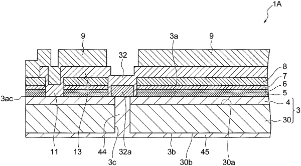
1. A field effect transistor comprising:
a substrate including a main surface and a back surface;
a semiconductor region on the main surface, the semiconductor region including an inactive region and an active region;
a gate electrode, a source electrode, and a drain electrode on the active region;
a drain pad being on the inactive region and electrically connected to the drain electrode; and
a drain guard on and in contact with the inactive region of the semiconductor region, the drain guard being apart from the drain pad,
wherein the drain guard is in a non-conductive state with respect to the gate electrode, the source electrode and the drain electrode.
|