| CPC H01L 23/552 (2013.01) [H01L 21/56 (2013.01); H01L 23/3107 (2013.01); H01L 23/4952 (2013.01); H01L 24/48 (2013.01); H01L 24/85 (2013.01); H01L 2224/48245 (2013.01); H01L 2224/85035 (2013.01); H01L 2224/85203 (2013.01); H01L 2224/85205 (2013.01)] | 20 Claims |
|
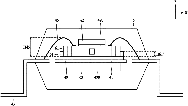
1. A package structure, comprising:
a mounting pad having a mounting surface;
a semiconductor chip disposed on the mounting surface of the mounting pad,
wherein the semiconductor chip comprises:
a first surface;
a second surface opposite to the first surface and facing the mounting surface; and
a third surface connecting the first surface and the second surface;
a first magnetic field shielding, comprising:
a first portion proximal to the third surface of the semiconductor chip, wherein the first portion has a first height calculated from the mounting surface to a top surface; and
a second portion distal to the semiconductor chip, has a second height calculated from the mounting surface to a position at a surface facing away from the mounting surface, wherein the second height is less than the first height, wherein the second portion has an inclined sidewall.
|