| CPC H01L 23/544 (2013.01) [H01L 23/481 (2013.01); H01L 25/0657 (2013.01); H01L 2223/54426 (2013.01); H01L 2225/06513 (2013.01); H01L 2225/06541 (2013.01); H01L 2225/06586 (2013.01); H01L 2225/06593 (2013.01)] | 20 Claims |
|
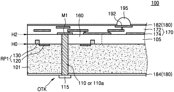
1. A through-silicon via (TSV) key for overlay measurement, the TSV key comprising:
a first TSV extending through at least a portion of a substrate in a first direction that is perpendicular to a top surface of the substrate; and
at least one ring pattern, which is spaced apart from and surrounds the first TSV in a second direction that is parallel to the top surface of the substrate, the at least one ring pattern being arranged in a layer that is lower than a top surface of the first TSV in the first direction,
wherein an inner measurement point corresponds to the first TSV, an outer measurement point corresponds to the at least one ring pattern, and the inner measurement point and the outer measurement point are arranged to provide an overlay measurement of a TSV, and
wherein the first TSV is not electrically operated and the at least one ring pattern is an insulating film.
|