| CPC H01L 23/5384 (2013.01) [H01L 21/486 (2013.01); H01L 21/76807 (2013.01); H01L 23/5386 (2013.01)] | 20 Claims |
|
1. A semiconductor device, comprising:
a first substrate including a first junction portion; and
a second substrate including a second junction portion, the second junction portion being joined to the first junction portion,
wherein the first substrate further includes:
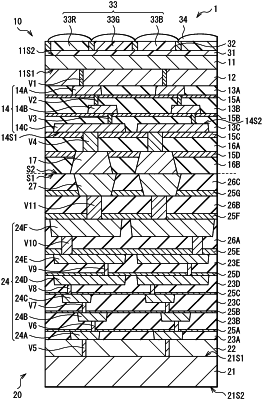
a first multilayer wiring layer in which one surface of a first wiring line faces a first insulating layer and another surface of the first wiring line opposed to the one surface of the first wiring line is in contact with a second insulating layer,
wherein the first insulating layer is provided between the first junction portion and the second insulating layer,
wherein the first multilayer wiring layer is electrically coupled to the first junction portion by a via of the first insulating layer,
wherein the first wiring line is formed closest to a junction surface with the second substrate, and
wherein the second insulating layer has a lower relative dielectric constant than a relative dielectric constant of the first insulating layer.
|