| CPC H01L 23/5381 (2013.01) [H01L 23/5383 (2013.01); H01L 28/20 (2013.01); H01L 28/40 (2013.01); H01L 23/5384 (2013.01); H01L 24/16 (2013.01); H01L 2224/16225 (2013.01)] | 20 Claims |
|
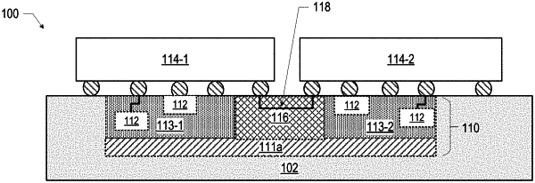
1. A microelectronic assembly, comprising:
a substrate having a surface;
a first die on the surface of the substrate;
a second die on the surface of the substrate;
a first interconnect area in the substrate located under the first die;
a second interconnect area in the substrate located under the second die
a bridge, embedded in the substrate under a portion of the first die and a portion of the second die, wherein the bridge includes a bridge substrate and one or more routing layers for signal routing between the first die and the second die, wherein the first interconnect area and the second interconnect area are on the bridge substrate and surround the one or more routing layers; and
a plurality of capacitors located in the first interconnect area and in the second interconnect area, wherein one or more first capacitors of the plurality of capacitors are connected to at least one other capacitor in the plurality of capacitors and one or more second capacitors of the plurality of the capacitors are not connected to another capacitor in the plurality of capacitors, wherein the first die is connected to the one or more first capacitors of the plurality of capacitors.
|
|
8. A microelectronic assembly, comprising:
a substrate having a surface;
a first die on the surface of the substrate;
a second die on the surface of the substrate;
a first interconnect area in the substrate located under the first die;
a second interconnect area in the substrate located under the second die;
a bridge, embedded in the substrate under a portion of the first die and a portion of the second die, wherein the bridge includes a bridge substrate and one or more routing layers for signal routing between the first die and the second die, wherein the first interconnect area and the second interconnect area are on the bridge substrate and surround the one or more routing layers; and
a plurality of capacitors located in the first interconnect area and in the second interconnect area, wherein the first die is connected to one or more first capacitors of the plurality of capacitors and is not connected to one or more second capacitors of the plurality of the capacitors.
|
|
15. An integrated circuit (IC) package, comprising:
a package substrate having a surface;
a first die on the surface of the package substrate;
a second die on the surface of the package substrate;
a first bridge interconnect area located under the first die, embedded in the package substrate, having a plurality of capacitors, wherein one or more first capacitors of the plurality of capacitors are connected to at least one other capacitor in the plurality of capacitors and one or more second capacitors of the plurality of the capacitors are not connected to another capacitor in the plurality of capacitors;
a second bridge interconnect area located under the second die, embedded in the package substrate, having a plurality of third capacitors connected to each other; and
a third bridge interconnect area, embedded in the package substrate under a portion of the first die and a portion of the second die and between the first bridge interconnect area and the second bridge interconnect area, wherein the third bridge interconnect area includes conductive pathways for signal routing between the first die and the second dies, wherein the first bridge interconnect area and the second bridge interconnect area surround the third bridge interconnect area.
|