US 11,749,599 B2
Dual thickness fuse structures
John J. Pekarik, Underhill, VT (US); Anthony K. Stamper, Burlington, VT (US); and Vibhor Jain, Essex Junction, VT (US)
Assigned to GLOBALFOUNDRIES INC., Malta, NY (US)
Filed by GLOBALFOUNDRIES INC., Grand Cayman (KY)
Filed on Nov. 13, 2020, as Appl. No. 17/97,432.
Application 17/097,432 is a division of application No. 15/975,041, filed on May 9, 2018, granted, now 10,910,308.
Prior Publication US 2021/0066194 A1, Mar. 4, 2021
Int. Cl. H01L 23/52 (2006.01); H01L 23/525 (2006.01); H01L 21/768 (2006.01); H01L 23/00 (2006.01); H01L 23/62 (2006.01)
CPC H01L 23/5258 (2013.01) [H01L 21/76843 (2013.01); H01L 23/573 (2013.01); H01L 23/62 (2013.01); H01L 24/16 (2013.01)] 20 Claims
OG exemplary drawing
 
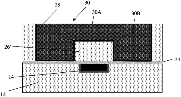
1. A method comprising: depositing an insulator material on an underlying substrate; patterning the insulator material to form adjacent openings in the insulator material thereby exposing the underlying substrate; patterning the insulator material which recesses an upper portion of the insulator material between the adjacent openings to form a single bump that extends into each of and is between the adjacent openings in the insulator material; depositing conductive material over the single bump and in the adjacent openings; and planarizing the conductive material to form a continuous wiring structure comprising a thin laser fuse portion and thicker overpass wiring structure on a same wiring level.