| CPC H01L 23/49838 (2013.01) [H01L 21/486 (2013.01); H01L 21/4857 (2013.01); H01L 23/49811 (2013.01); H01L 23/49822 (2013.01)] | 20 Claims |
|
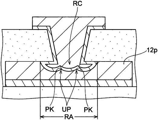
1. A wiring substrate, comprising:
a conductor pad;
an insulating layer formed on the conductor pad such that the insulating layer is covering the conductor pad and has a through hole; and
a bump formed on the conductor pad such that the bump is formed in the through hole penetrating through the insulating layer,
wherein the conductor pad is formed such that the conductor pad has a connecting surface connected to the bump, a concave part formed on the connecting surface of the conductor pad to the bump, and a convex part formed in the concave part.
|