| CPC H01L 23/49833 (2013.01) [H01L 23/3121 (2013.01); H01L 23/32 (2013.01); H01L 23/49816 (2013.01); H01L 24/16 (2013.01); H01L 24/73 (2013.01); H01L 25/105 (2013.01); H01L 2224/16227 (2013.01); H01L 2224/32227 (2013.01); H01L 2224/73204 (2013.01); H01L 2225/1023 (2013.01); H01L 2225/1058 (2013.01)] | 20 Claims |
|
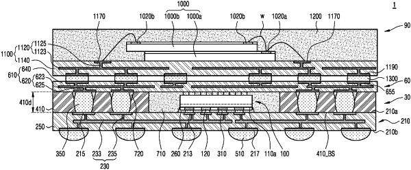
1. A lower semiconductor package of a package-on-package type semiconductor package, the lower semiconductor package comprising:
a package substrate;
a semiconductor chip having a first surface facing the package substrate, a second surface opposite to the first surface mounted on the package substrate;
a chip connecting terminal disposed between the semiconductor chip and the package substrate and configured to connect the semiconductor chip to the package substrate;
conductive pillars arranged on the package substrate to at least partially surround the semiconductor chip; and
a dam structure configured to cover the conductive pillars on the package substrate and having a first opening at least partially surrounding the semiconductor chip,
wherein a level of a top surface of the dam structure is higher than a level of the second surface of the semiconductor chip.
|