| CPC H01L 23/49822 (2013.01) [H01L 23/49827 (2013.01); H01L 23/49894 (2013.01); H05K 1/115 (2013.01); H05K 3/34 (2013.01); H05K 3/3452 (2013.01); H05K 3/4015 (2013.01); H05K 3/4644 (2013.01); H01L 2224/16225 (2013.01); H01L 2224/32225 (2013.01); H01L 2224/73204 (2013.01); H05K 2201/095 (2013.01); H05K 2201/098 (2013.01); H05K 2203/02 (2013.01)] | 5 Claims |
|
1. A wiring substrate device comprising:
a wiring substrate;
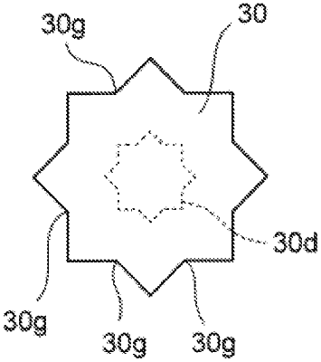
a plurality of terminals each of which is provided upright on the wiring substrate and has a lower end provided on the wiring substrate, an upper end opposite to the lower end, a side surface extending between the lower end and the upper end, and a narrowed part in the side surface between the lower end and the upper end, the narrowed part having a narrow portion having a smallest width of the terminal, as seen from a cross sectional view, in a width direction of the terminal, the width direction being orthogonal to a height direction of the terminal, the height direction of the terminal extending between the lower end and the upper end; and
a plurality of solders each of which has a melting point lower than the terminals and covers a surface of the corresponding terminal,
wherein the side surface of each of the terminals defines a plurality of grooves therein, the plurality of grooves extending, in the height direction of the terminal, between the lower end and the upper end, the plurality of grooves each reaching both the lower end and the upper end, and the plurality of grooves passing through the narrowed part.
|