| CPC H01L 23/481 (2013.01) [H01L 29/0649 (2013.01); H01L 29/0665 (2013.01); H01L 29/66795 (2013.01); H01L 29/785 (2013.01)] | 20 Claims |
|
1. A method of manufacturing a semiconductor device, the method comprising:
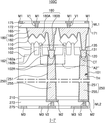
preparing a device structure having a substrate having a first surface and a second surface opposite each other, and being provided with an active region at the first surface, wherein the active region has a plurality of active fins extending in a first direction, a device isolation region defining the plurality of active fins on the first surface of the substrate, a buried conductive line buried in the device isolation region and a portion of the active region, and extending in the first direction, an insulating isolation film including a first portion between the device isolation region and the buried conductive line and a second portion between the active region and the buried conductive line, an interlayer insulating layer disposed on the device isolation region, and covering the buried conductive line, and a contact structure connected to the buried conductive line through the interlayer insulating layer;
forming a through-hole extending toward the first surface of the substrate from the second surface of the substrate, wherein the second portion of the insulating isolation film is exposed on a bottom surface of the through-hole;
forming an insulating liner on an inner surface of the through-hole, and the second portion of the insulating isolation film;
partially removing the insulating liner and the second portion of the insulating isolation film to expose a portion of the buried conductive line, wherein the exposed portion of the buried conductive line extends beyond a bottom surface of the buried conductive line toward the second surface of the substrate; and
forming a through-via in the through-hole to contact a bottom surface of the exposed portion of the buried conductive line and a side surface of the exposed portion of the buried conductive line, wherein the side surface of the exposed portion of the buried conductive line is adjacent to the bottom surface of the exposed portion of the buried conductive line.
|