| CPC H01L 23/481 (2013.01) [H01L 21/76898 (2013.01); H01L 23/528 (2013.01); H01L 25/0657 (2013.01); H01L 27/0886 (2013.01); H01L 24/02 (2013.01); H01L 24/05 (2013.01); H01L 24/06 (2013.01); H01L 2224/02381 (2013.01); H01L 2224/0401 (2013.01); H01L 2224/0557 (2013.01); H01L 2224/05569 (2013.01); H01L 2224/0603 (2013.01); H01L 2224/06181 (2013.01); H01L 2225/06513 (2013.01); H01L 2225/06544 (2013.01)] | 20 Claims |
|
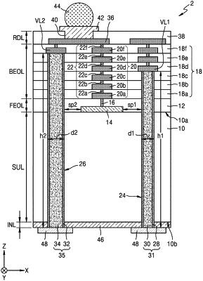
1. A semiconductor device comprising:
a semiconductor substrate;
an integrated circuit layer on the semiconductor substrate;
first to nth metal wiring layers (where n is a positive integer) sequentially stacked on the semiconductor substrate and the integrated circuit layer;
a first through via structure extending in a vertical direction toward the semiconductor substrate from a first via connection metal wiring layer, and passing through the semiconductor substrate, the first via connection metal wiring layer being one of the second to nth metal wiring layers other than the first metal wiring layer; and
a second through via structure being apart from the first through via structure, extending in a vertical direction toward the semiconductor substrate from a second via connection metal wiring layer, and passing through the semiconductor substrate, the second via connection metal wiring layer being one of the second to nth metal wiring layers other than the first metal wiring layer.
|