US 11,749,583 B2
Electronic package and method for manufacturing the same
Chih-Hsien Chiu, Taichung (TW); Siang-Yu Lin, Taichung (TW); Wen-Jung Tsai, Taichung (TW); Chia-Yang Chen, Taichung (TW); and Chien-Cheng Lin, Taichung (TW)
Assigned to SILICONWARE PRECISION INDUSTRIES CO., LTD., Taichung (TW)
Filed by SILICONWARE PRECISION INDUSTRIES CO., LTD., Taichung (TW)
Filed on Jul. 19, 2021, as Appl. No. 17/379,289.
Claims priority of application No. 110118447 (TW), filed on May 21, 2021.
Prior Publication US 2022/0375822 A1, Nov. 24, 2022
Int. Cl. H01L 23/42 (2006.01); H01L 23/367 (2006.01); H01L 23/16 (2006.01); H01L 21/56 (2006.01); H01L 23/31 (2006.01)
CPC H01L 23/42 (2013.01) [H01L 21/561 (2013.01); H01L 23/16 (2013.01); H01L 23/3128 (2013.01); H01L 23/367 (2013.01)] 30 Claims
OG exemplary drawing
 
1. An electronic package, comprising:
a plurality of electronic components; and
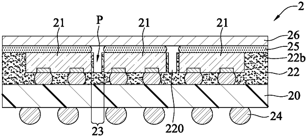
an encapsulation layer encapsulating the plurality of electronic components, wherein a spacer is defined in the encapsulation layer and located between at least two adjacent electronic components of the plurality of electronic components, and a recess is formed in the spacer and used as a thermal insulation area, and wherein a thermal conductivity of the thermal insulation area is less than 0.02 W/mk.