| CPC H01L 21/76829 (2013.01) [H01L 21/76802 (2013.01); H01L 21/76826 (2013.01); H01L 21/76828 (2013.01); H01L 21/76877 (2013.01); H01L 23/53295 (2013.01)] | 20 Claims |
|
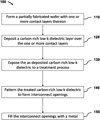
1. A method, comprising:
depositing, using an electron beam (e-beam) assisted deposition method, a dielectric layer on a surface of a substrate at a temperature between about 24° C. and about 300° C., wherein the dielectric layer, as-deposited by the e-beam assisted deposition method, comprises a dielectric constant lower than about 3.9 and a carbon atomic concentration between about 15% and about 20%;
forming pores in the dielectric layer;
treating the dielectric layer having pores in a gas mixture comprising additives to increase the carbon atomic concentration;
etching the dielectric layer having pores to form openings; and
filling the openings with a conductive material to form conductive structures.
|