| CPC H01L 21/67144 (2013.01) [H01L 21/67132 (2013.01); H01L 24/75 (2013.01); H05K 13/0419 (2018.08); H01L 21/6838 (2013.01); H01L 2224/7565 (2013.01); H05K 13/0409 (2018.08)] | 7 Claims |
|
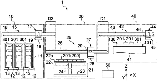
1. A bonding apparatus comprising:
an electronic component supply module comprising a carrier tape and a first transfer part adjacent to the carrier tape, the first transfer part taking out an electronic component from the carrier tape and transferring the taken-out electronic component from the electronic component supply module;
a die supply module comprising a pickup part and a second transfer part adjacent to the pickup part, the picking part picking up a semiconductor die from a wafer bonded to a dicing sheet of the picking part by pushing up the semiconductor die, and the second transfer part transferring out the picked-up semiconductor die from the die supply module; and
a bonding module bonding at least one of the semiconductor die supplied by the die supply module and the electronic component supplied by the electronic component supply module to a substrate,
wherein the second transfer part is a common transfer path and receives the electronic component transferred from the first transfer part, both the electronic component and the semiconductor die are transferred to the bonding module through the second transfer part, the first transfer part is an independent transfer path, one of the electronic component and the semiconductor die is transferred out to the common transfer path through the first transfer part, and a region where the first transfer part and the second transfer part overlap is set in the die supply module.
|