| CPC H01L 21/565 (2013.01) [H01L 21/0337 (2013.01); H01L 21/31116 (2013.01); H01L 21/31144 (2013.01)] | 20 Claims |
|
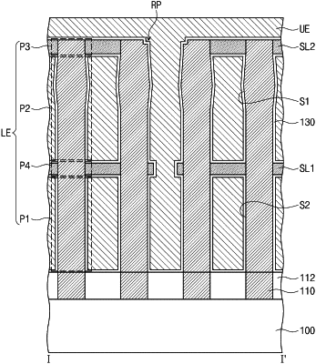
1. A semiconductor device, comprising:
a bottom electrode on a substrate, the bottom electrode having a pillar shape;
a first support layer on a sidewall of the bottom electrode;
a second support layer above the first support layer and on the sidewall of the bottom electrode; and
a dielectric layer covering the sidewall and a top surface of the bottom electrode,
wherein the bottom electrode includes:
a lower segment between the first support layer and the second support layer; and
an upper segment between the lower segment and the second support layer, the upper segment having a sidewall that protrudes from a sidewall of the lower segment such that a center of the sidewall has a sharp point, and
wherein the bottom electrode has a concave segment which is a portion recessed from the top surface of the bottom electrode.
|