| CPC H01L 21/4839 (2013.01) [H01L 21/561 (2013.01); H01L 21/568 (2013.01); H01L 24/13 (2013.01); H01L 24/16 (2013.01); H01L 24/81 (2013.01); H01L 2224/13147 (2013.01); H01L 2224/16245 (2013.01); H01L 2224/81411 (2013.01); H01L 2224/81424 (2013.01); H01L 2224/81439 (2013.01); H01L 2224/81444 (2013.01); H01L 2224/81447 (2013.01); H01L 2224/81455 (2013.01); H01L 2224/81457 (2013.01); H01L 2224/81466 (2013.01); H01L 2224/81469 (2013.01); H01L 2224/81481 (2013.01); H01L 2224/81484 (2013.01)] | 29 Claims |

|
1. A method of making a quad flat no-lead (QFN), dual flat no-lead (DFN) or small outline no-lead (SON) package without a leadframe, comprising:
disposing at least two semiconductor chips face-up on a temporary carrier, the at least two semiconductor chips each comprising conductive stumps over an active layer of each of the at least two semiconductor chips;
disposing a first layer of encapsulant in a single step around four side surfaces of each of the at least two semiconductor chips, over the active layer of each of the at least two semiconductor chips, and around the conductive stumps;
planarizing the first layer of encapsulant over the active layer of each of the at least two semiconductor chips to create a planar surface comprising exposed ends of the conductive stumps and an exposed encapsulant surface;
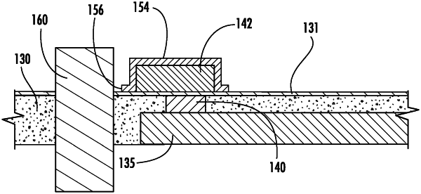
forming a first conductive layer and first vertical conductive contacts over the planar surface and configured to be electrically coupled with the conductive stumps of the at least two semiconductor chips;
disposing a second layer of encapsulant over the first layer of encapsulant, the first conductive layer and the first vertical conductive contacts;
forming a first photoresist over the second layer of encapsulant with openings formed through the first photoresist over the first vertical conductive contacts;
forming conductive pads in the form of land pads or bumps within the openings and then removing the first photoresist;
forming a second photoresist over the second layer of encapsulant with conductive pad openings formed through the second photoresist over the conductive pads;
forming a solderable metal system (SMS) or applying an organic solderability preservative (OSP) over the conductive pads to resist oxidation over at least a portion of the conductive pads; and
cutting through the second layer of encapsulant around at least one of the at least two semiconductor chips to form an outline of a package.
|