| CPC H01L 21/4807 (2013.01) [H01L 21/52 (2013.01); H01L 23/367 (2013.01); H01L 23/3731 (2013.01)] | 15 Claims |
|
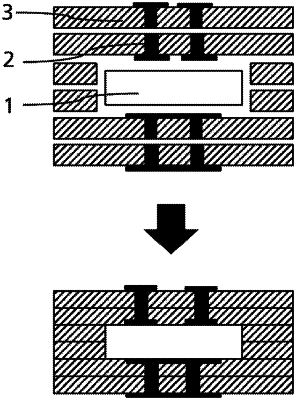
1. A method of manufacturing a power semiconductor component arrangement or a power semiconductor component housing, the method comprising:
providing an arrangement that comprises at least one semiconductor component, at least one element for an electrical contacting of the at least one semiconductor component, and a plurality of layer-shaped unsintered ceramic substrates, wherein the plurality of layer-shaped unsintered ceramic substrates are arranged at least partially around the at least one semiconductor component and the at least one element for the electrical contacting the at least one semiconductor component, and
subjecting the arrangement to a sintering process in which the plurality of layer-shaped unsintered ceramic substrates are converted into a sintered ceramic single layer or multilayer substrate and simultaneously an electrical connection of the at least one semiconductor component to the at least one element for the electrical contacting of the at least one semiconductor component takes place and a mechanical connection of the at least one semiconductor component and of the at least one element for the electrical contacting of the at least one semiconductor component to the ceramic single layer or multilayer substrate takes place;
wherein the arrangement has at least one insulation layer that is arranged on the at least one semiconductor component, wherein during the sintering process, a mechanical bonding of the at least one semiconductor component and of the at least one element for the electrical contacting of the at least one semiconductor component to the ceramic single-layer or multilayer substrate takes place at least in part via the at least one insulation layer.
|