| CPC H01L 21/0337 (2013.01) [H01L 21/0332 (2013.01); H01L 21/31144 (2013.01); H01L 21/76802 (2013.01); H01L 21/76877 (2013.01); H01L 23/528 (2013.01)] | 20 Claims |

|
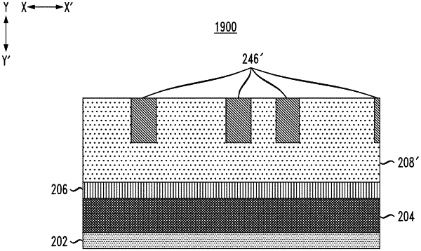
1. A method of forming a semiconductor structure, comprising:
forming a dielectric layer;
forming a plurality of mandrel lines over the dielectric layer;
forming a plurality of non-mandrel lines over the dielectric layer between adjacent ones of the plurality of mandrel lines utilizing self-aligned double patterning;
forming at least one spacer-merge region, the at least one spacer-merge region extending from a first portion of a first one of the plurality of mandrel lines to a second portion of a second one of the plurality of mandrel lines in a first direction and covering at least a portion of one or more of the plurality of non-mandrel lines between the first mandrel and the second mandrel in a second direction orthogonal to the first direction; and
forming a plurality of trenches in the dielectric layer by transferring a pattern of (i) the plurality of mandrel lines and (ii) portions of the plurality of non-mandrel lines outside the at least one spacer-merge region.
|