| CPC H01J 37/32522 (2013.01) [H01J 37/321 (2013.01); H01J 37/3299 (2013.01); H01J 37/32651 (2013.01); H01J 37/3211 (2013.01); H01J 37/32119 (2013.01); H01L 21/67069 (2013.01)] | 10 Claims |
|
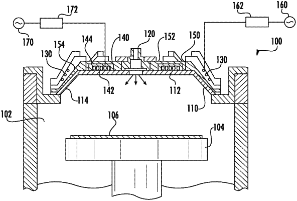
1. A plasma processing apparatus, comprising:
a processing chamber;
a pedestal located in the processing chamber configured to support a w orkpiece during processing;
a dielectric window forming at least a portion of the processing chamber, the dielectric window comprising a first portion and a second portion;
a first inductive coupling element and a second inductive coupling element located proximate the dielectric window, the first inductive coupling element being adjacent the first portion of the dielectric w indow and the second inductive coupling element being adjacent the second portion of the dielectric window, the first and second inductive coupling elements configured to generate a plasma in the processing chamber when energized with radio frequency (RF) energy;
a first Faraday shield located betw een the first inductive coupling element and the processing chamber;
a second Faraday shield located betw een the second inductive coupling element and the processing chamber; and
at least one temperature control element in thermal communication w ith the second Faraday shield;
wherein the at least one temperature control element comprises a thin film heating element disposed on a surface of the second Faraday shield, and w herein each of the at least one temperature control element is in direct contact with the second portion of the dielectric window and spaced apart from the first portion of the dielectric window, the thin film heating element providing a cooling path to transfer heat from the dielectric window to the second Faraday shield w hen the thin film heating element is not heated, thereby acting as a heat sink to facilitate cooling of the dielectric window.
|