| CPC H01G 9/2031 (2013.01) [H01G 9/2013 (2013.01); H01G 9/2022 (2013.01); H01G 9/2059 (2013.01); H01G 9/2077 (2013.01); H01L 31/022441 (2013.01)] | 20 Claims |
|
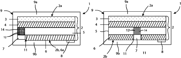
1. A photovoltaic device comprising:
a solar cell unit comprising stacked layers, including:
a working electrode layer comprising a porous light-absorbing layer arranged at a top side of the solar cell unit,
a first conducting layer for extracting photo-generated electrons from the light-absorbing layer, wherein the light-absorbing layer is arranged on top of the first conducting layer,
a porous substrate layer made of an insulating material, wherein the first conducting layer is formed on a top side of the porous substrate layer,
a counter electrode layer including a second conducting layer arranged at a bottom side of the solar cell unit that is parallel to the top side of the solar cell unit, wherein the second conducting layer is formed on a bottom side of the porous substrate layer and each of the light-absorbing layer, the first conducting layer, the porous substrate layer, and second conducting layer are parallel to the top and bottom sides of the solar cell unit so that the second conducting layer is spaced apart from the first conducting layer in a direction extending normal from the top side of the solar cell unit to the bottom side of the solar cell unit with the porous substrate layer between the first and second conducting layers, and wherein the solar cell unit further comprises a conducting medium for transferring charges between the second conducting layer and the light-absorbing layer, wherein the porosity of the porous substrate layer enables the conducting medium to pass through the porous substrate layer,
a first conductor below the porous substrate layer and the first conducting layer in the direction extending normal from the top side of the solar cell unit to the bottom side of the solar cell unit, and the first conductor is in electrical contact with the first conducting layer,
a second conductor below the counter electrode layer in the direction extending normal from the top side of the solar cell unit to the bottom side of the solar cell unit, and the second conductor in electrical contact with the second conducting layer, and
an encapsulation encapsulating the solar cell unit and comprising an at least partly transparent top sheet covering the top side of the solar cell unit and a bottom sheet covering the bottom side of the solar cell unit, wherein the second conductor is arranged between the second conducting layer and the bottom sheet of the encapsulation at the bottom side of the solar cell unit, and the first conductor is arranged between the porous substrate layer and the bottom sheet at the bottom side of the solar cell unit,
wherein the first conductor is electrically insulated from the second conducting layer, and
wherein a part of the porous substrate layer comprises conducting material disposed between the first conductor and the first conducting layer to provide electrical contact between the first conductor and the first conducting layer, wherein the conducting material is separate from the conducting medium and comprises conducting particles accommodated in pores of said part of the porous substrate layer, wherein the conducting particles form a conducting path through the porous substrate layer between the first conductor and the first conducting layer.
|