| CPC G11C 19/184 (2013.01) [H01L 27/124 (2013.01); H01L 27/1222 (2013.01); H01L 27/1225 (2013.01); G09G 2310/0275 (2013.01); G09G 2310/0286 (2013.01); H01L 27/0248 (2013.01)] | 6 Claims |
|
1. A semiconductor device comprising:
first to tenth transistors having a same channel type,
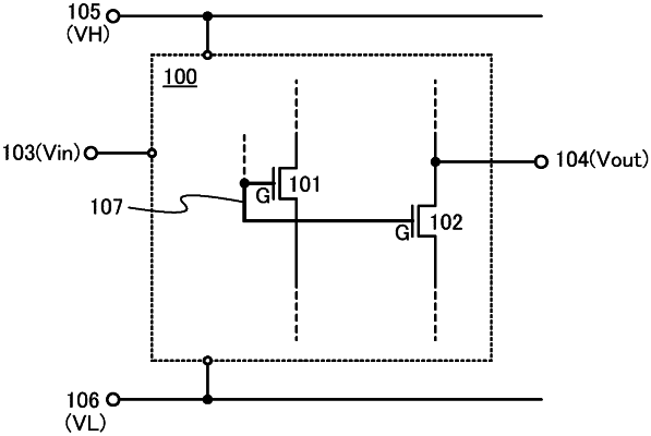
wherein one of a source and a drain of the first transistor is electrically connected to a first wiring, and the other of the source and the drain of the first transistor is electrically connected to a second wiring,
wherein one of a source and a drain of the second transistor is electrically connected to the second wiring, and the other of the source and the drain of the second transistor is electrically connected to a third wiring,
wherein one of a source and a drain of the third transistor is electrically connected to a fourth wiring, and the other of the source and the drain of the third transistor is electrically connected to a gate of the seventh transistor,
wherein one of a source and a drain of the fourth transistor is electrically connected to the gate of the seventh transistor, and the other of the source and the drain of the fourth transistor is electrically connected to a fifth wiring,
wherein one of a source and a drain of the fifth transistor is electrically connected to the fourth wiring, and the other of the source and the drain of the fifth transistor is electrically connected to a gate of the first transistor,
wherein one of a source and a drain of the sixth transistor is electrically connected to the fourth wiring, the other of the source and the drain of the sixth transistor is electrically connected to one of a source and a drain of the seventh transistor, and a gate of the sixth transistor is electrically connected to the gate of the first transistor,
wherein one of a source and a drain of the eighth transistor is electrically connected to the fourth wiring, the other of the source and the drain of the eighth transistor is electrically connected to one of a source and a drain of the ninth transistor, and a gate of the eighth transistor is electrically connected to the gate of the first transistor,
wherein the other of the source and the drain of the ninth transistor is electrically connected to a sixth wiring,
wherein one of a source and a drain of the tenth transistor is electrically connected to the gate of the first transistor,
wherein a first conductive layer serving as the gate of the first transistor is electrically connected to a third conductive layer serving as a gate of the third transistor through a second conductive layer, and
wherein the second wiring is configured to transmit a signal output from a circuit including the first to tenth transistors.
|