| CPC G11C 16/3459 (2013.01) [G11C 16/08 (2013.01); G11C 16/10 (2013.01); G11C 16/24 (2013.01); G11C 16/26 (2013.01); G11C 16/30 (2013.01)] | 12 Claims |
|
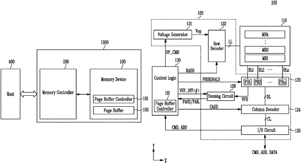
1. A memory device comprising:
a memory cell coupled to a bit line and a word line;
a page buffer coupled to the bit line, and configured to output a bit line voltage to the bit line in response to a page buffer sensing signal; and
control logic configured to:
output, to the page buffer, a signal increased from a first voltage level at a first time of a precharge period to a second voltage level at a second time of the precharge period, as the page buffer sensing signal,
in response to the second voltage level being less than a target voltage level, output, to the page buffer, a pulse signal having the target voltage level at a third time of the precharge period, as the page buffer sensing signal, and
output a control signal to provide a program voltage to the word line after the precharge period.
|