| CPC G11C 16/32 (2013.01) [G06F 3/0611 (2013.01); G06F 3/0659 (2013.01); G06F 3/0688 (2013.01); G11C 16/08 (2013.01); H03L 7/08 (2013.01)] | 20 Claims |
|
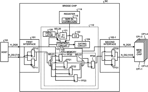
1. A semiconductor integrated circuit comprising:
a register configured to store numerical information, the numerical information representing a size of first data to be transferred between a first device and a second device;
a first interface circuit configured to receive, from the first device, a first timing signal for transfer of the first data;
an oscillation circuit configured to generate a first clock;
a phase-locked loop circuit configured to generate a second clock;
a control circuit configured to:
in response to start of toggling of the first timing signal, input the first timing signal to the phase-locked loop circuit and count the number of toggles of the first timing signal, and
input the first clock to the phase-locked loop circuit when a count of the number of toggles of the first timing signal matches a value corresponding to the numerical information; and
a second interface circuit configured to transmit the first timing signal or a second timing signal to the second device, the second timing signal corresponding to the second clock generated by the phase-locked loop circuit with reference to the first clock.
|