US 11,749,344 B2
Three-dimensional vertical nor flash thin-film transistor strings
Eli Harari, Saratoga, CA (US)
Assigned to SUNRISE MEMORY CORPORATION, San Jose, CA (US)
Filed by SUNRISE MEMORY CORPORATION, San Jose, CA (US)
Filed on Aug. 4, 2021, as Appl. No. 17/394,249.
Application 15/837,734 is a division of application No. 15/343,332, filed on Nov. 4, 2016, granted, now 9,842,651, issued on Dec. 12, 2017.
Application 17/394,249 is a continuation of application No. 17/121,509, filed on Dec. 14, 2020, granted, now 11,127,461.
Application 17/121,509 is a continuation of application No. 17/005,744, filed on Aug. 28, 2020, granted, now 10,902,917, issued on Jan. 26, 2021.
Application 17/005,744 is a continuation of application No. 16/503,229, filed on Jul. 3, 2019, granted, now 10,790,023, issued on Sep. 29, 2020.
Application 16/503,229 is a continuation of application No. 16/280,407, filed on Feb. 20, 2019, granted, now 10,395,737, issued on Aug. 27, 2019.
Application 16/280,407 is a continuation of application No. 16/107,732, filed on Aug. 21, 2018, granted, now 10,249,370, issued on Apr. 2, 2019.
Application 16/107,732 is a continuation of application No. 15/837,734, filed on Dec. 11, 2017, granted, now 10,096,364, issued on Apr. 19, 2018.
Application 15/343,332 is a continuation in part of application No. 15/248,420, filed on Aug. 26, 2016, granted, now 10,121,553, issued on Nov. 6, 2018.
Application 15/248,420 is a continuation in part of application No. 15/220,375, filed on Jul. 26, 2016, granted, now 9,892,800, issued on Feb. 13, 2018.
Claims priority of provisional application 62/363,189, filed on Jul. 15, 2016.
Claims priority of provisional application 62/260,137, filed on Nov. 25, 2015.
Claims priority of provisional application 62/235,322, filed on Sep. 30, 2015.
Prior Publication US 2021/0366544 A1, Nov. 25, 2021
Int. Cl. G11C 16/04 (2006.01); H01L 23/528 (2006.01); G11C 16/28 (2006.01); H01L 29/08 (2006.01); H01L 29/16 (2006.01); H01L 29/04 (2006.01); H01L 29/06 (2006.01); H01L 29/786 (2006.01); G11C 16/10 (2006.01); H01L 29/10 (2006.01); H01L 29/51 (2006.01); H01L 29/66 (2006.01); H01L 21/02 (2006.01); H01L 21/3213 (2006.01); H01L 21/768 (2006.01); H01L 29/423 (2006.01); H01L 21/28 (2006.01); G11C 11/56 (2006.01); G11C 16/26 (2006.01); G11C 16/34 (2006.01); H01L 27/06 (2006.01); H01L 29/792 (2006.01); H01L 49/02 (2006.01); H10B 43/10 (2023.01); H10B 43/27 (2023.01); H10B 43/35 (2023.01); H10B 43/40 (2023.01)
CPC G11C 16/0466 (2013.01) [G11C 11/5628 (2013.01); G11C 11/5635 (2013.01); G11C 16/0416 (2013.01); G11C 16/0483 (2013.01); G11C 16/0491 (2013.01); G11C 16/10 (2013.01); G11C 16/26 (2013.01); G11C 16/28 (2013.01); G11C 16/3427 (2013.01); H01L 21/0217 (2013.01); H01L 21/02164 (2013.01); H01L 21/02532 (2013.01); H01L 21/02595 (2013.01); H01L 21/32133 (2013.01); H01L 21/76892 (2013.01); H01L 23/528 (2013.01); H01L 27/0688 (2013.01); H01L 28/00 (2013.01); H01L 29/04 (2013.01); H01L 29/0649 (2013.01); H01L 29/0847 (2013.01); H01L 29/1037 (2013.01); H01L 29/16 (2013.01); H01L 29/40117 (2019.08); H01L 29/4234 (2013.01); H01L 29/513 (2013.01); H01L 29/518 (2013.01); H01L 29/6675 (2013.01); H01L 29/66833 (2013.01); H01L 29/78642 (2013.01); H01L 29/7926 (2013.01); H10B 43/10 (2023.02); H10B 43/27 (2023.02); H10B 43/35 (2023.02); H10B 43/40 (2023.02)] 31 Claims
OG exemplary drawing
 
1. A process for creating a memory structure over a planar surface of a semiconductor substrate, comprising:
depositing a first insulation layer over the planar surface;
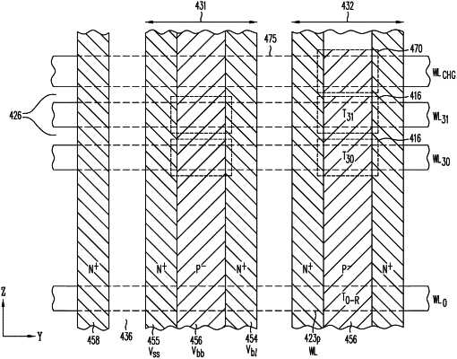
over the first insulation layer, forming a plurality of material layers each separated from another by an intervening insulator layer, each material layer comprising either a conductive material or a sacrificial material;
etching a plurality of trenches through the material layers and the intervening insulator layers until reaching the planar surface, each trench extending in depth along a first direction substantially normal to the planar surface;
conformally depositing a charge-trapping layer over the sidewalls of the trenches;
conformally depositing a lightly doped polysilicon of a first conductivity over the surface of the charge-trapping layers on the sidewalls of the trenches;
filling the trenches with a dielectric material; and
forming in each filled trench first and second shafts, each shaft having the lightly doped polysilicon as a portion of its sidewalls; and
filling each shaft with a heavily doped polysilicon material of a second conductivity opposite the first conductivity.