| CPC G11C 13/0026 (2013.01) [G11C 13/0028 (2013.01)] | 20 Claims |
|
1. An apparatus, comprising:
a memory array comprising a plurality of memory cells disposed between at least two access lines of a plurality of access lines of the memory array, wherein:
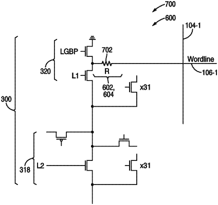
a first access line of the plurality of access lines comprises a first electrical current path configured to provide access to a target memory cell of the plurality of memory cells on a first side of the target memory cell, wherein the first electrical current path comprises a first parasitic electrical resistance associated with accessing the target memory cell; and
a second access line of the plurality of access lines comprises a second electrical current path configured to provide access to the target memory cell on a second side of the target memory cell, wherein a first one or more transistors are coupled to the second access line between at least two memory cells of the plurality of memory cells and configured to provide a first compensatory resistance when providing access to the target memory cell, and wherein the second electrical current path comprises a second parasitic electrical resistance associated with accessing the target memory cell.
|