| CPC G11C 11/005 (2013.01) [G11C 11/1673 (2013.01); G11C 11/1675 (2013.01); G11C 11/419 (2013.01)] | 21 Claims |
|
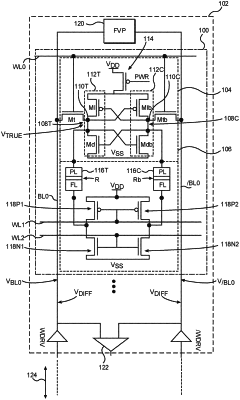
1. A memory bit cell circuit, comprising:
a bit line;
a static random-access memory (SRAM) bit cell circuit, comprising:
a storage circuit, comprising:
a true inverter circuit comprising:
a true input node;
a true output node comprising a true storage node;
a true power node coupled to a supply voltage rail; and
a true ground node coupled to a ground voltage rail; and
a complement inverter circuit comprising:
a complement input node coupled to the true output node of the true inverter circuit;
a complement output node comprising a complement storage node coupled to the true input node of the true inverter circuit;
a complement power node coupled to a high voltage rail; and
a complement ground node coupled to a low voltage rail; and
a first access circuit coupled to the true output node and the bit line; and
a non-volatile memory (NVM) bit cell circuit comprising:
a NVM device coupled between the complement output node and a first node; and
a second access circuit coupled to the first node and the bit line,
wherein the NVM device is a magnetic random-access memory (MRAM) device configured to, in response to the second access circuit coupling the first node to the bit line, store a first binary NVM data based on conducting a first current in a first direction between the bit line and the complement storage node or conducting a second current in a second direction between the bit line and the complement storage node and wherein the supply voltage rail is configured to receive a supply voltage, the ground voltage rail is configured to receive a ground voltage, the high voltage rail is configured to receive a higher voltage than the supply voltage, the low voltage rail is configured to receive a lower voltage than the ground voltage, and in response to the second access circuit coupling the first node to the bit line, the complement inverter circuit is configured to conduct one of the first current in the first direction and the second current in the second direction through the NVM device.
|