| CPC G11C 8/06 (2013.01) [G06F 3/06 (2013.01); G06F 13/1689 (2013.01); G11C 7/10 (2013.01); G11C 7/1045 (2013.01); G11C 7/22 (2013.01); G11C 8/10 (2013.01); G11C 8/18 (2013.01); G11C 11/4076 (2013.01); G11C 7/1057 (2013.01)] | 20 Claims |
|
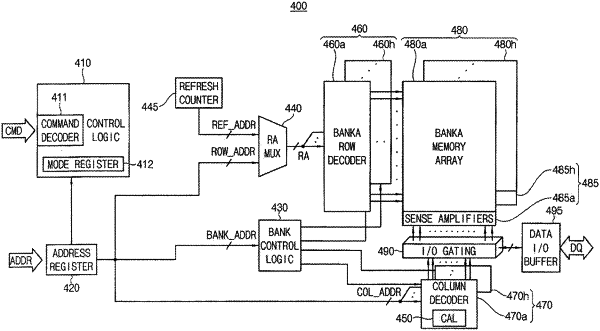
1. A dynamic random access memory (DRAM) device operating in synchronization with a clock signal, the DRAM device comprising:
a memory cell array including a plurality of memory cells; and
a control logic configured to receive a command which is split into a first portion and a second portion, the first portion of the command including a first portion of an address and the second portion of the command including a second portion of the address, the first portion and the second portion of the address, combined together, indicating a location of memory cells operating in response to the command,
wherein the control logic, during a first operating mode, receives the first portion of the command and the second portion of the command at first and second rising edges of the clock signal respectively in which the second rising edge follows the first rising edge after a first number of clock cycles, and during a second operating mode, receives the first portion of the command and the second portion of the command at third and fourth rising edges of the clock signal respectively in which the fourth rising edge follows the third rising edge after a second number of clock cycles, and the first number and the second number are different from each other.
|