| CPC G09G 5/10 (2013.01) [G09G 3/3233 (2013.01); G09G 2320/045 (2013.01); G09G 2320/0646 (2013.01)] | 20 Claims |
|
1. A display device comprising:
a display panel including a plurality of pixels to display an image; and
a panel control circuit wherein the panel control circuit comprises:
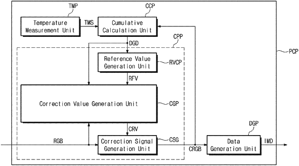
a correction circuit configured to receive image signals of a current frame period to generate correction image signals of the current frame period; and
a cumulative calculation circuit configured to accumulate the correction images signals of the current frame period and generate degradation data based on accumulated correction image signals generated by accumulating previous correction image signals of a prior frame period to the cumulative calculation circuit,
wherein the correction circuit is configured to determine reference data from the degradation data and generate the correction image signals of the current frame period by correcting the image signals of the current frame period by correcting the image signals of the current frame period to have a target luminance that is changed based on the reference data, and
wherein the panel control circuit generates image data of the current frame period for application to the pixels based on the correction image signals of the current frame period.
|