| CPC G09G 3/3677 (2013.01) [G09G 3/3688 (2013.01); G09G 2300/0842 (2013.01); G09G 2310/0267 (2013.01); G09G 2310/0286 (2013.01); G09G 2310/061 (2013.01); G09G 2330/021 (2013.01)] | 16 Claims |
|
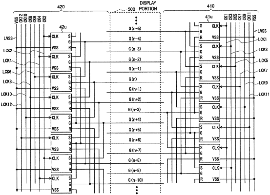
1. A scanning signal line drive circuit configured to drive a plurality of scanning signal lines arranged on a display portion of a display device, the scanning signal line drive circuit comprising:
a plurality of unit circuits cascade-connected to each other and configured to operate as a shift register based on a multiphase clock signal,
wherein the multiphase clock signal includes a plurality of clock signals cyclically corresponding to the plurality of unit circuits,
each of the plurality of unit circuits is a bistable circuit corresponding to one of the plurality of scanning signal lines, receives a corresponding clock signal among the plurality of clock signals as an input clock signal, receives an output signal of a predetermined unit circuit of preceding stages or a first input signal applied from the outside of the shift register as a set signal, receives an output signal of a predetermined unit circuit of a succeeding stage or a second input signal applied from the outside of the shift register as a reset signal, and includes
a first internal node configured to selectively hold voltages of a first and second logic levels,
a set circuit configured to apply the voltage of the first logic level to the first internal node in response to the set signal,
a reset circuit configured to apply the voltage of the second logic level to the first internal node in response to the reset signal, and
an output circuit configured to generate an output signal of a logic level corresponding to the input clock signal and apply the output signal to a corresponding scanning signal line when the voltage held in the first internal node is at the first logic level,
the predetermined unit circuit of the succeeding stage configured to output a signal input as the reset signal is a unit circuit of k stages after an own stage, k being a natural number satisfying i−j≤k≤i−1 when the predetermined unit circuit of the preceding stages configured to output the signal input as the set signal is a unit circuit of j stages before the own stage and the number of phases of the multiphase clock signal is i,
the reset circuit includes a reset transistor including a first conduction terminal connected to the first internal node, a second conduction terminal configured to receive the voltage of the second logic level, and a control terminal configured to receive the reset signal,
the reset signal input to each of the plurality of unit circuits is an output signal of the unit circuit of k stages after the own stage when the own stage is not one of unit circuits of last k stages in the plurality of unit circuits and is the second input signal when the own stage is any of the unit circuits of the last k stages,
the second input signal input to each of the unit circuits of the last k stages is a signal configured to turn to an active state only for a predetermined period after an output signal of the own stage changes from the active state to a non-active state,
each of the unit circuits of the last k stages includes a compensation circuit including a compensation transistor including a first conduction terminal connected to the first internal node, the compensation transistor turning on or off according to a compensation control signal being one of the set signal of the own stage or the output signal of the own stage, and
the compensation circuit in each of the unit circuits of the last k stages is configured to
turn the compensation transistor to an off state or apply the voltage of the first logic level to the first internal node during a period when the first internal node is to hold the voltage of the first logic level, and
turn the compensation transistor to an on state or the off state according to the voltage of the compensation control signal and apply the voltage of the second logic level to the first internal node via the compensation transistor when the compensation transistor is in the on state during a period when the first internal node is to hold the voltage of the second logic level.
|