| CPC G09G 3/3648 (2013.01) [G09G 3/3674 (2013.01); G09G 2310/0297 (2013.01)] | 23 Claims |
|
1. An active matrix substrate including a display region having a plurality of pixel regions and a peripheral region located in a periphery of the display region, the active matrix substrate comprising:
a substrate;
a plurality of gate bus lines and a plurality of source bus lines on the substrate;
a source driver disposed in the peripheral region and including a plurality of output terminals;
a plurality of signal output lines each connected to a corresponding one of the plurality of output terminals of the source driver; and
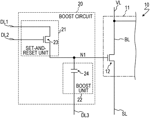
a demultiplexer circuit which includes a plurality of unit circuits supported by the substrate and which is disposed in the peripheral region, wherein
each of the plurality of unit circuits of the demultiplexer circuit distributes a display signal from one signal output line of the plurality of signal output lines to n source bus lines of the plurality of source bus lines, where n is an integer larger than or equal to 2,
each of the plurality of unit circuits includes
n branch lines connected to the one signal output line, and
n switching TFTs each connected to a corresponding one of the n branch lines, the n switching TFTs being configured to perform individual on/off control of electrical connections of the n branch lines to the n source bus lines,
the demultiplexer circuit further includes a plurality of boost circuits each configured to boost a voltage applied to a gate electrode of a corresponding one of the n switching TFTs,
each of the plurality of boost circuits includes
a set-and-reset unit configured to perform a set operation of pre-charging a node connected to the gate electrode and a reset operation of resetting potential of the node at different timings, and
a boost unit configured to perform a boost operation of boosting the potential of the node pre-charged by the set operation performed by the set-and-reset unit,
the demultiplexer circuit includes a first drive signal line and a second drive signal line via which a first drive signal and a second drive signal are respectively supplied to the set-and-reset unit,
the set-and-reset unit includes a setting-and-resetting TFT having a gate electrode connected to the second drive signal line, a source electrode, and a drain electrode, one of the source electrode and the drain electrode being connected to the first drive signal line, and the other of the source electrode and the drain electrode being connected to the node,
the setting-and-resetting TFT is configured to perform the set operation and the reset operation at different timings,
the setting-and-resetting TFT is in an ON state at a time of performing the set operation and at a time of performing the reset operation, and
the set-and-reset unit does not include any TFT other than the setting-and-resetting TFT.
|