| CPC G09G 3/342 (2013.01) [G09G 2300/0426 (2013.01); G09G 2330/028 (2013.01)] | 19 Claims |
|
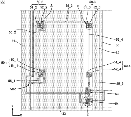
1. A light-emitting substrate, comprising a base and a plurality of light-emitting units disposed on the base, a light-emitting unit including:
a driving voltage terminal;
a main driver chip pad group;
a plurality of main light-emitting element pad groups connected in series, both ends of the plurality of main light-emitting element pad groups being coupled to the driving voltage terminal and the main driver chip pad group;
at least one spare light-emitting element pad group, each spare light-emitting element pad group being connected in parallel with one of the plurality of main light-emitting element pad groups to constitute a pad unit; and
a plurality of first lines, wherein the plurality of first lines are disposed between the driving voltage terminal and the main driver chip pad group, and sequentially connect the plurality of main light-emitting element pad groups; the plurality of first lines include two first lines connected to the main light-emitting element pad group in the pad unit, and the two first lines are a first connection line and a second connection line; wherein
the main light-emitting element pad group and the spare light-emitting element pad group in the pad unit each includes an anode and a cathode, the anode pads of the spare light-emitting element pad group and the main light-emitting element pad group are both disposed on the first connection line, and the cathode pads of the spare light-emitting element pad group and the main light-emitting element pad group are both disposed on the second connection line.
|