| CPC G09G 3/3291 (2013.01) [G09G 3/3233 (2013.01); G09G 3/3266 (2013.01); G09G 2300/0426 (2013.01); G09G 2300/0439 (2013.01); G09G 2300/0809 (2013.01); G09G 2310/08 (2013.01)] | 10 Claims |
|
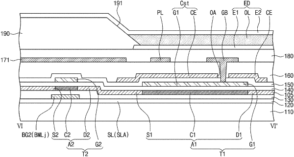
1. An organic light emitting display device comprising:
a substrate including a display area and a non-display area;
a light emitting diode disposed in the display area;
a transistor comprising a channel, a first electrode disposed over the channel, and a second electrode disposed under the channel;
a voltage line disposed in the non-display area; and
a first driving voltage line disposed in the display area;
wherein the second electrode of the transistor overlaps with the first electrode of the transistor when viewed in a plan view with the channel interposed between the first electrode and the second electrode, and the second electrode is electrically connected to the voltage line through a contact hole disposed in the non-display area, and
wherein the first driving voltage line overlaps with the second electrode in the display area.
|