| CPC G09G 3/3275 (2013.01) [G09G 3/3233 (2013.01); G09G 3/3266 (2013.01); G09G 2310/0248 (2013.01); G09G 2310/0286 (2013.01)] | 18 Claims |
|
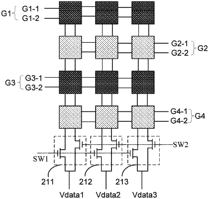
1. A signal control apparatus for a display apparatus, the display apparatus comprising M rows by N columns of pixel driving circuits arranged in an array, wherein the M pixel driving circuits of each column of pixel driving circuits are grouped into at least a first group of pixel driving circuits and a second group of pixel driving circuits, M and N each being an integer and N being larger than 2, and the first group of pixel driving circuits are connected to a first data line to receive a data signal, and the second group of pixel driving circuits are connected to a second data line to receive a data signal, the signal control apparatus comprising:
a phase shifting circuit configured to provide a scanning signal to a pixel driving circuit, wherein the phase shifting circuit includes a phase shifter and a first register, and wherein the phase shifter is connected to an input terminal of the first register, an output terminal of the first register is connected to at least one of M scanning signal terminals, and the M scanning signal terminals correspond to M pixel driving circuits in the same column of pixel driving circuits one by one,
wherein one of the scanning signals of adjacent two pixel driving circuits in the same column of pixel driving circuits is shifted with respect to the other one of the scanning signals of the adjacent two pixel driving circuits in the same column of pixel driving circuits by a factor smaller than a duration of a data signal writing phase of each pixel driving circuit.
|