| CPC G09G 3/3266 (2013.01) [G09G 3/3275 (2013.01); H10K 59/131 (2023.02); G09G 2310/0278 (2013.01); G09G 2310/062 (2013.01)] | 20 Claims |
|
1. A display device comprising:
a pixel connected to each of a first scan line, a second scan line, and a data line;
a scan driver to supply a first scan signal to the first scan line and a second scan signal to the second scan line;
a data driver to supply a data signal to the data line; and
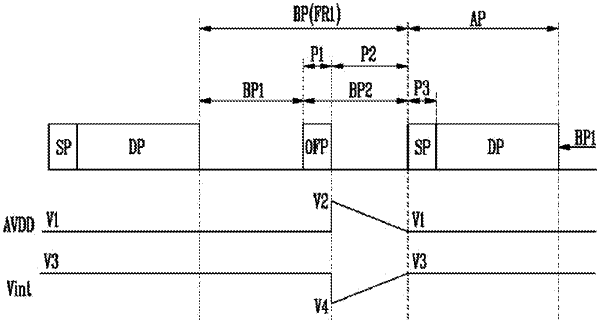
a controller to receive image data, and to control the scan driver and the data driver to drive the pixel to display an image during a frame based on the image data, the frame being divided into an active period and a blank period,
wherein the scan driver is configured to output the first scan signal in the blank period when the blank period is greater than a reference time duration,
wherein the reference time duration is substantially the same as a first blank period corresponding to a maximum frame rate of the display device,
wherein the pixel comprises a light-emitting element, a first transistor connected between a first driving power source and the light-emitting element and including a gate electrode connected to a first node, a third transistor to supply a reference voltage to a second node at which the first transistor and the light-emitting element are connected in response to the first scan signal supplied to a gate electrode thereof,
wherein the blank period comprises the first blank period and a second blank period following the first blank period when the blank period is greater than the reference time duration,
wherein the reference voltage gradually increases during the second blank period.
|
|
12. A display device comprising:
a pixel connected to each of a first scan line, a second scan line, and a data line;
a scan driver to supply a first scan signal to the first scan line and a second scan signal to the second scan line;
a data driver to supply a data signal to the data line; and
a controller to receive image data, and to control the scan driver and the data driver to drive the pixel to display an image during a frame based on the image data, the frame being divided into an active period and a blank period,
wherein the scan driver is configured to output the first scan signal in the blank period when the blank period is greater than a reference time duration, and
wherein the reference time duration is substantially the same as a first blank period corresponding to a maximum frame rate of the display device,
wherein the blank period comprises the first blank period and a second blank period following the first blank period when the blank period is greater than the reference time duration, and
wherein the scan driver is configured to output the first scan signal in the second blank period.
|
|
17. A display device comprising:
a plurality of pixels, each connected to a power supply line, a data line, and a scan line;
a scan driver to supply a scan signal to the scan line;
a data driver to supply a data signal to the data line;
a power supply to generate at least one supply voltage for at least one of the data driver or the scan driver; and
a controller to receive image data, and to control the scan driver, the data driver, and the power supply to drive the plurality of pixels to display an image during a frame based on the image data, the frame being divided into an active period and a blank period,
wherein the at least one supply voltage comprises at least one of:
at least one source driving voltage connected to at least one of the data driver, the at least one source driving voltage being adjustable to control the data signal based on a time duration of the blank period, or
at least one reference voltage connected to a source electrode of a pixel driving transistor of at least one of the plurality of pixels through the power supply line, the at least one reference voltage being adjustable based on the time duration of the blank period.
|