| CPC G09G 3/3266 (2013.01) [G09G 3/3233 (2013.01); G09G 2310/0286 (2013.01); G09G 2310/0291 (2013.01); G09G 2310/08 (2013.01); G09G 2320/043 (2013.01); G09G 2330/021 (2013.01); G09G 2354/00 (2013.01)] | 15 Claims |
|
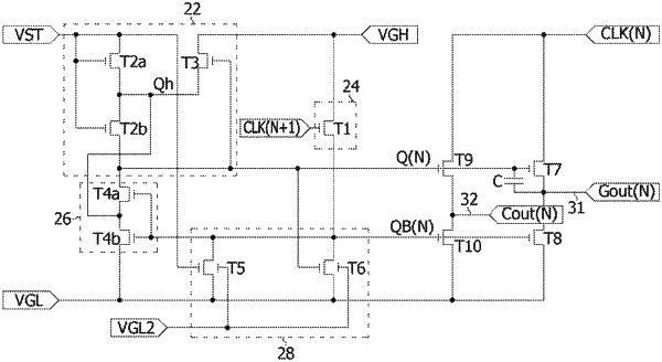
1. A gate driving circuit comprising:
a shift register including signal transmitters configured to receive a start pulse and a shift clock, the signal transmitters being connected in a cascade structure to sequentially generate a gate pulse,
wherein an Nth signal transmitter among the signal transmitters includes:
a VST node to which the start pulse or a carry signal from a preceding signal transmitter is applied;
one or more CLK nodes to which the shift clock is inputted;
a VDD node to which a high-potential driving voltage is applied;
a VSS node to which a low-potential reference voltage is applied;
a first control node configured to control a first pull-up transistor;
a second control node configured to control a first pull-down transistor;
a first charge controller configured to charge the first control node in response to the voltage of the VST node;
a second charge controller configured to charge the second control node using a first transistor that is turned on in response to an (N+1)th clock generated following an Nth clock;
a first discharge controller configured to discharge the first control node in a charging period of the second control node; and
a second discharge controller configured to discharge the second control node when the voltage of the VST node is a high voltage or during a charging period of the first control node, where N is a positive integer,
wherein the shift clock includes:
the Nth clock inputted to a first CLK node, the (N+1)th clock inputted to a second CLK node following the Nth clock, and another dock inputted to a third CLK node following the (N+1)th clock, and
wherein the low-potential reference voltage includes:
a first low-potential reference voltage applied to a first VSS node; and
a second low-potential reference voltage set to be lower than the first low-potential reference voltage and applied to a second VSS node.
|