| CPC G09G 3/3266 (2013.01) [G09G 3/3233 (2013.01); G09G 2300/0819 (2013.01); G09G 2300/0861 (2013.01); G09G 2310/08 (2013.01); G09G 2320/0233 (2013.01); G09G 2360/16 (2013.01)] | 20 Claims |
|
1. A display apparatus comprising:
a pixel part comprising a plurality of pixels, each of the plurality of pixels being configured to receive a first scan signal from a first scan line from among first scan lines and an emission signal from an emission line from among emission lines; and
a scan driver connected to the first scan lines and the emission lines, and configured to output the first scan signal to the first scan lines and the emission signal to the emission lines,
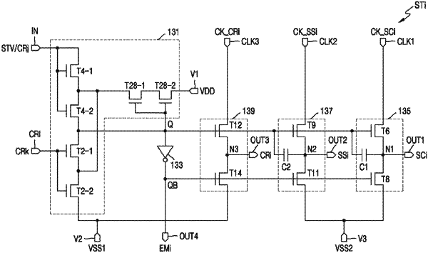
wherein the scan driver comprises a plurality of stages, and each of the plurality of stages comprises an inverter connected between a first control node and a second control node,
wherein the inverter is configured to invert a voltage level of a voltage of the first control node, and to supply a voltage output from the inverter to the second control node, and
wherein the scan driver is configured to output the first scan signal according to the voltage of the first control node and to output the voltage of the second control node as the emission signal.
|