| CPC G09G 3/3258 (2013.01) [G09G 3/3291 (2013.01); G09G 2300/0819 (2013.01)] | 19 Claims |
|
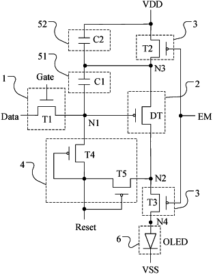
1. A pixel driving circuit, comprising:
a data-writing circuit, a driving circuit, a light-emitting control circuit, a compensation circuit, and a storage circuit, wherein:
the data-writing circuit is coupled to the driving circuit for writing a data signal to the driving circuit;
the driving circuit is coupled to a first power supply end and a light-emitting sub-circuit through the light-emitting control circuit for inputting a driving current to the light-emitting sub-circuit according to the data signal under control of the light-emitting control circuit;
the compensation circuit is coupled to the driving circuit;
the storage circuit is coupled between the first power supply end and the driving circuit; and
the data-writing circuit and the compensation circuit together comprise at least two transistors, wherein, in the data-writing circuit and the compensation circuit, at least one transistor is a low temperature polysilicon transistor, and at least one transistor is an oxide transistor; wherein:
the data-writing circuit is connected to a data signal end, a gate driving signal end and a first node, for transmitting a signal of the data signal end to the first node in response to a signal of the gate driving signal end;
the driving circuit is connected to the first node, a second node, and a third node, for inputting the driving current to the second node according to a signal of the first node;
the light-emitting control circuit is connected to the third node, the second node, the first power supply end, a fourth node and an enable signal end, for transmitting a signal of the first power supply end to the third node in response to a signal of the enable signal end, and for transmitting a signal of the second node to the fourth node in response to the signal of the enable signal end;
the compensation circuit is connected to the first node, the second node and a reset signal end, for transmitting a signal of the reset signal end to the first node and the second node in response to the signal of the reset signal end;
the storage circuit comprises a first storage circuit and a second storage circuit;
the first storage circuit is connected between the first node and the third node;
the second storage circuit is connected between the third node and the first power supply end; and
the light-emitting sub-circuit is connected between the fourth node and a second power supply end.
|