| CPC G09G 3/3233 (2013.01) [G01N 11/02 (2013.01); G01N 27/4161 (2013.01); G01N 27/4166 (2013.01); G01N 33/18 (2013.01); G09G 3/3266 (2013.01); G09G 3/3283 (2013.01); H01L 27/1222 (2013.01); H10K 59/1216 (2023.02); H10K 59/131 (2023.02); G09G 2300/0426 (2013.01); G09G 2300/0819 (2013.01); G09G 2300/0823 (2013.01); G09G 2300/0852 (2013.01); G09G 2300/0861 (2013.01); G09G 2320/0214 (2013.01); G09G 2320/0219 (2013.01); G09G 2320/0238 (2013.01); H01L 27/124 (2013.01); H01L 27/1225 (2013.01); H01L 27/1255 (2013.01); H01L 29/7869 (2013.01); H01L 29/78675 (2013.01); H10K 59/1213 (2023.02)] | 10 Claims |
|
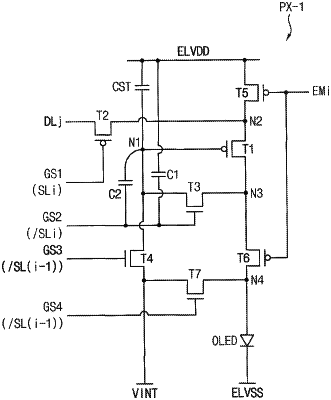
1. An organic light emitting display device, comprising;
a first supply voltage line;
a second supply voltage line;
an initialization voltage line;
an organic light emitting diode;
a first transistor, a second transistor, and a third transistor electrically connected in series between the first supply voltage line and the second supply voltage line, wherein the first transistor includes a first portion of a first active pattern made of a first semiconductor material, the second transistor includes a second portion of the first active pattern, and the third transistor includes a third portion of the first active pattern;
a fourth transistor electrically connected between a data line and a first electrode of the second transistor, wherein the fourth transistor includes a fourth portion of the first active pattern;
a fifth transistor electrically connected between a gate electrode of the second transistor and a second electrode of the second transistor, wherein the fifth transistor includes a first portion of a second active pattern made of a second semiconductor material that differs from the first semiconductor material; and
a capacitor electrically connected to the gate electrode of the second transistor,
wherein the second active pattern is electrically connected to the gate electrode of the second transistor through a first connector,
wherein the second active pattern is electrically connected to the first active pattern through a second connector, and
wherein the second active pattern is electrically connected to the initialization voltage line through a third connector.
|