| CPC G09G 3/3233 (2013.01) [G09G 2300/0819 (2013.01); G09G 2300/0842 (2013.01); G09G 2310/08 (2013.01); G09G 2320/0257 (2013.01); G09G 2320/045 (2013.01); G09G 2330/021 (2013.01)] | 20 Claims |
|
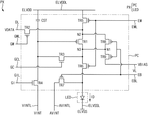
1. A pixel comprising:
a first switching transistor including a first terminal to which a bias power supply voltage is applied, a second terminal connected to a first node, and a gate terminal to which a light emitting element initialization signal is applied;
a second switching transistor including a first terminal connected to the first node, a second terminal connected to a second node, and a gate terminal to which the light emitting element initialization signal is applied;
a driving transistor including a first terminal connected to the second node, a second terminal connected to a third node, and a gate terminal; and
a light emitting element including a first terminal electrically connected to the driving transistor,
wherein the first node, which connects the first and second switching transistors to each other, is connected to the third node, and
the bias power supply voltage is applied to the second and third nodes.
|