| CPC G09G 3/3233 (2013.01) [G09G 3/3266 (2013.01); G09G 3/2007 (2013.01); G09G 2300/0426 (2013.01); G09G 2300/0819 (2013.01); G09G 2300/0842 (2013.01); G09G 2310/0294 (2013.01); G09G 2310/08 (2013.01); G09G 2320/0252 (2013.01)] | 18 Claims |
|
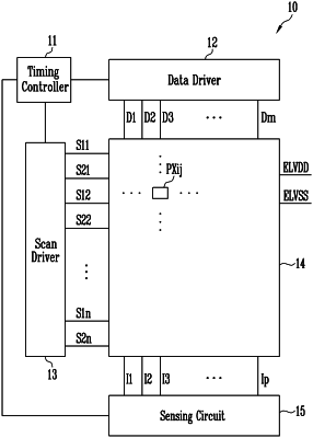
1. A display device comprising:
pixels connected to scan lines; and
a scan driver, which supplies scan signals to the scan lines,
wherein the scan driver includes active stages having first output terminals connected to the scan lines, and
wherein each of the active stages includes:
a scan output circuit, which outputs a scan clock signal to a first output terminal when a voltage of a first active node is at a logic high level, and, outputs a scan signal of a turn-off level to the first output terminal when a voltage of a second active node or a first carry signal is at a logic high level; and
a carry output circuit, which outputs a carry clock signal to a second output terminal when the voltage of the first active node is at the logic high level, and, outputs a carry signal of a turn-off level to the second output terminal when the voltage of the second active node or the first carry signal is at the logic high level,
wherein intervals between pulses of the carry clock signal generated during one frame period are the same, and
wherein at least two of intervals between pulses of the scan clock signal generated during the one frame period are different from each other,
wherein each of the active stages further includes:
an inverter, which charges the second active node with the voltage of the logic high level when the voltage of the first active node is at a logic low level and a first control signal is at a logic high level, and
a feedback circuit, which charges a third active node with the first control signal when the voltage of the first active node is at the logic high level,
wherein the feedback circuit includes:
a twelfth transistor having a first electrode, which receives the first control signal, a gate electrode connected to the first active node, and a second electrode connected to the third active node.
|