| CPC G09G 3/3233 (2013.01) [G09G 3/2007 (2013.01); H10K 59/1315 (2023.02); G09G 2300/0426 (2013.01); G09G 2300/0465 (2013.01); G09G 2300/0842 (2013.01); G09G 2310/0202 (2013.01); G09G 2310/08 (2013.01); G09G 2320/0223 (2013.01); G09G 2320/0233 (2013.01); G09G 2330/08 (2013.01)] | 37 Claims |
|
1. A display substrate, comprising:
a base substrate;
a pixel row, comprising a plurality of sub-pixels on the base substrate and arranged along a first direction,
a first scan line and a second scan line, located on the base substrate and extended along the first direction,
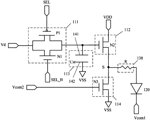
wherein each of the sub-pixels comprises a pixel circuit, and the pixel circuit comprises a data writing sub-circuit, a storage sub-circuit, and a driving sub-circuit;
the data writing sub-circuit comprises a first control electrode, a second control electrode, a first terminal and a second terminal, the first control electrode and the second control electrode of the data writing sub-circuit are respectively configured to receive a first control signal and a second control signal, the first terminal of the data writing sub-circuit is configured to receive a data signal, and the second terminal of the data writing sub-circuit is electrically connected to a first terminal of the storage sub-circuit, and is configured to transmit the data signal to the first terminal of the storage sub-circuit in response to the first control signal and the second control signal;
the driving sub-circuit comprises a control terminal, a first terminal and a second terminal, the control terminal of the driving sub-circuit is electrically connected with the first terminal of the storage sub-circuit, the first terminal of the driving sub-circuit is configured to receive a first power supply voltage, the second terminal of the driving sub-circuit is configured to be connected with a light-emitting element, and the driving sub-circuit is configured to drive the light-emitting element to emit light in response to a voltage of the first terminal of the storage sub-circuit;
the first scan line is electrically connected with the first control electrode of the data writing sub-circuit of each of the plurality of sub-pixels to provide the first control signal; the second scan line is electrically connected with the second control electrode of the data writing sub-circuit of each of the plurality of sub-pixels to provide the second control signal; and
a resistance of the first scan line is the same as a resistance of the second scan line, and an area of an orthographic projection of the first scan line on the base substrate is same as an area of an orthographic projection of the second scan line on the base substrate.
|