| CPC G09G 3/3208 (2013.01) [G02F 1/133528 (2013.01); H10K 30/865 (2023.02); H10K 50/844 (2023.02); H10K 50/8426 (2023.02); H10K 50/865 (2023.02); H10K 50/87 (2023.02); H10K 59/32 (2023.02); H10K 59/40 (2023.02); H10K 77/10 (2023.02); G02F 1/3505 (2021.01); H10K 50/86 (2023.02); H10K 59/12 (2023.02)] | 12 Claims |
|
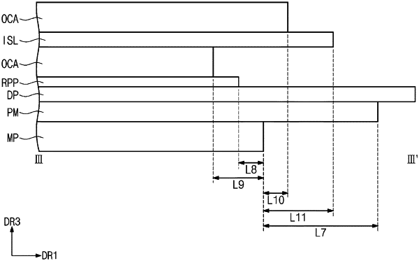
1. A display device, comprising:
a display panel, in which a display region comprising a plurality of organic light emitting devices and a non-display region adjacent to the display region are defined;
a protection film disposed below the display panel;
a first adhesive layer contacting a bottom surface of the protection film;
a supporting layer comprising a metallic material, at least overlapping the entire display region, and contacting the first adhesive layer;
an input-sensing unit disposed on the display panel;
an anti-reflection unit disposed on the input-sensing unit; and
a window panel disposed on the input-sensing unit.
|