| CPC G09G 3/32 (2013.01) [G09G 2310/08 (2013.01)] | 7 Claims |
|
1. An electro-optical device comprising
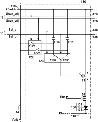
a plurality of pixel circuits provided corresponding to intersections between a data line and a plurality of scanning lines, each of the plurality of pixel circuits including a first selector, a second selector, a first capacitance element, a second capacitance element, a drive transistor, and a light-emitting element,
the drive transistor being configured to supply, to the light-emitting element, a current corresponding to a voltage of a gate node, wherein
in a first frame,
the plurality of scanning lines are selected sequentially,
the first selector in one pixel circuit of the plurality of pixel circuits electrically couples, when one scanning line corresponding to the one pixel circuit is selected, one end of the first capacitance element to the data line, and
the second selector in the one pixel circuit electrically couples one end of the second capacitance element to the gate node, and
in a second frame different from the first frame,
the plurality of scanning lines are selected sequentially,
the first selector in the one pixel circuit electrically couples, when the one scanning line is selected, one end of the second capacitance element to the data line, and
the second selector in the one pixel circuit electrically couples one end of the first capacitance element to the gate node.
|