| CPC G09G 3/32 (2013.01) [G09G 3/006 (2013.01); G09G 2300/0408 (2013.01); G09G 2310/0267 (2013.01); G09G 2310/0283 (2013.01); G09G 2310/0286 (2013.01)] | 20 Claims |
|
1. A display panel, comprising:
a plurality of signal pins comprising at least a start signal pin and a detection signal pin;
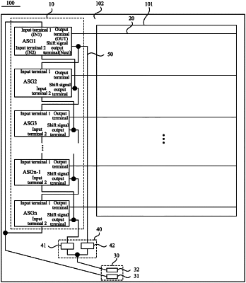
a scan driving circuit and a plurality of scan signal lines, wherein the scan driving circuit comprises N scan drive units disposed in a cascade manner, wherein N is a positive integer greater than or equal to 2; scan signal output terminals of the N scan drive units are electrically connected to the plurality of scan signal lines with a one-to-one correspondence; for each of the N scan drive units, a forward scan input terminal of a current-stage scan drive unit is electrically connected to a shift signal output terminal of a previous-stage scan drive unit of the current-stage scan drive unit, a backward scan input terminal of the current-stage scan drive unit is electrically connected to a shift signal output terminal of a next-stage scan drive unit of the current-stage scan drive unit, and a forward scan input terminal of a first-stage scan drive unit and a backward scan input terminal of an Nth-stage scan drive unit are both electrically connected to the start signal pin, wherein the current-stage scan drive unit is not the first-stage scan drive unit and not the Nth-stage scan drive unit; and
a first gating circuit comprising a first switch unit and a second switch unit, wherein an input terminal of the first switch unit is electrically connected to a scan signal detection terminal of the Nth-stage scan drive unit, an input terminal of the second switch unit is electrically connected to a scan signal detection terminal of the first-stage scan drive unit, an output terminal of the first switch unit and an output terminal of the second switch unit are both electrically connected to the detection signal pin; the first switch unit is configured to turn on in a forward scan detection stage and turn off in a backward scan detection stage, and the second switch unit is configured to turn on in the backward scan detection stage and turn off in the forward scan detection stage,
wherein the scan signal detection terminal of the Nth-stage scan drive unit is a shift signal output terminal of the Nth-stage scan drive unit or a scan signal output terminal of the Nth-stage scan drive unit, and the scan signal detection terminal of the first-stage scan drive unit is a shift signal output terminal of the first-stage scan drive unit or a scan signal output terminal of the first-stage scan drive unit.
|