| CPC G09G 3/20 (2013.01) [G11C 19/28 (2013.01); G09G 2300/0408 (2013.01); G09G 2300/08 (2013.01); G09G 2310/0243 (2013.01); G09G 2310/0267 (2013.01); G09G 2310/0286 (2013.01); G09G 2310/08 (2013.01)] | 16 Claims |
|
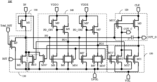
1. A gate driving circuit comprising multiple stages of shift registers, the multiple stages of shift registers comprising N first shift registers arranged alternately with N second shift registers,
wherein the N first shift registers are cascaded-coupled as N stages of first shift registers, and are configured to generate N first output signals under control of K first clock signals;
wherein the N second shift registers are cascaded-coupled as N stages of second shift registers, and are configured to generate N second output signals under a control of K second clock signals;
wherein K and N are both integers greater than 1, and K<N;
wherein an input signal terminal of an n-th stage of first shift register in the N stages of first shift registers is coupled to an output signal terminal of an (n−i)-th stage of first shift register in the N stages of first shift registers, and a reset signal terminal of the n-th stage of first shift register is coupled to an output signal terminal of an (n+j)-th stage of first shift register in the N stages of first shift registers;
wherein an input signal terminal of an n-th stage of second shift register in the N stages of second shift registers is coupled to an output signal terminal of an (n−i)-th stage of second shift register in the N stages of second shift registers, and a reset signal terminal of the n-th stage of second shift register is coupled to an output signal terminal of an (n+j)-th stage of second shift register in the N stages of second shift registers;
wherein n, i, and j are all integers greater than 0, K is an even number, 1<n<N, 1≤i≤K/2, and K/2+1≤j≤K−1; and
wherein K=6, i=3, and j=4.
|