| CPC G09G 3/20 (2013.01) [G09G 2310/0267 (2013.01); G09G 2310/0291 (2013.01); G09G 2330/021 (2013.01)] | 14 Claims |
|
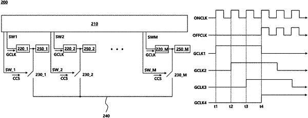
1. A gate driver circuit, comprising:
a control circuit configured to output gate clock signals and connection control signals;
a first buffer to receive a first gate clock signal from the control circuit and to output the first gate clock signal;
a second buffer to receive a second gate clock signal from the control circuit and to output the second gate clock signal;
a first charge sharing switch connected with an output end of the first buffer and controlled by the connection control signal; and
a second charge sharing switch connected with an output end of the second buffer, connected with the first charge sharing switch through a charge sharing line, and controlled by the connection control signal,
wherein the control circuit turns on the first charge sharing switch and the second charge sharing switch when the first gate clock signal and the second gate clock signal are respectively in different edge states.
|